Product Details
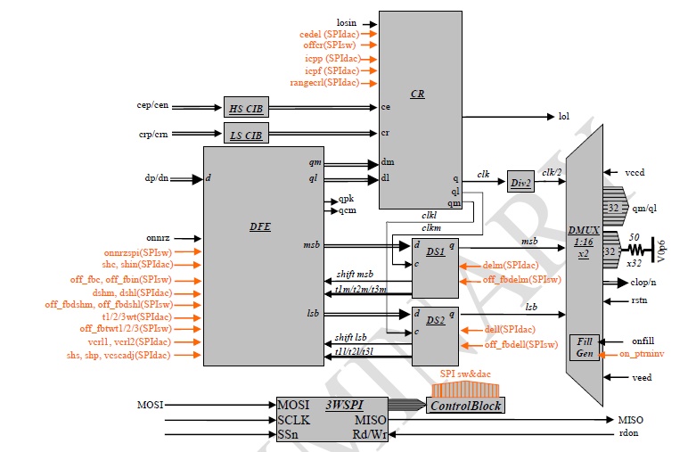
Fig. 1. Functional Block Diagram
The ASNT8763-KMT is an adjustable clock and data recovery (CDR) system for either NRZ or PAM3 signals. Its operational modes are controlled through the on-chip 3-wire SPI and/or
through external ports. The onnrz control (external analog port or SPI byte combined through 2- input logic OR function) must be set in accordance with the input signal type. An internal DFE is designed for optimal data reconstruction of the differential input signal dp/dn as well as for automatic conversion of the input signal into two pairs of binary signals that represent transitions either in the top (MSB) or the bottom (LSB) portions of the PAM3 signal.
The first two of the binary output signals of DFE go to the Clock Recovery (CR) block. CR can either let an external clock signal from the input cep/cen through or use the two NRZ data
signals from DFE along with the reference clock input signal crp/crn to generate a recovered clock signal which is phase-locked to input data. The other two output data signals from DFE are delivered to two identical Data Sample blocks (DS1 and DS2). DS1 reconstructs the MSB portion of the PAM3 signal by latching it with the clock signal provided by CR. Similarly, DS2 reconstructs the LSB portion of the PAM3 signal by latching it with the clock signal provided by CR. DS1 and DS2 also provide data shift feedback controls, tap weight feedback controls, and tap signals for DFE. Six tap signals are fed back to DFE to optimally shape its output signals. The tap weights and polarities are automatically set by three independent feedback loops.
The reconstructed data streams from DS1 and DS2 are demultiplexed by a dual demultiplexer 1- to-16 (DMX1:16×2) block and delivered to the output SSTL interface as single-ended signals qm00-qm15 and ql00-ql15 together with the corresponding low-speed differential SSTL clock clop/clon. The real data can be replaced by a pre-defined bit pattern generated inside the block. Most operational modes of the chip are controlled by the Control Block that communicates with an external computer through a high-speed 3-wire serial interface (3wSPI). The SPI is activated by active-low chip enable signal (SSn).The SPI can be forced by the active-low external signal rdon to read its internal registers without re-writing them. The SPI supply voltage can be controlled or adjusted through the v1p2 pin.
The part operates with a positive supply vcc = +3.3V for the main data paths and a positive supply vcc_vco = +3.3V for VCO, and additional positive supplies v4p3 = +4.3V for DFE. A
separate positive supply vccd=+1.2V is provided for the internal output CMOS circuitry. The additional termination supply v0p6=+0.6V with a bi-directional current is required for the output interface operation. The negative supply rails vee and veed should be both connected to external ground.