Product Details

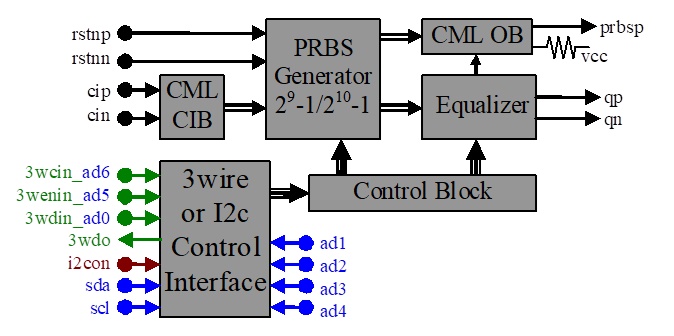
Fig.1 Functional Block Diagram
The ASNT8145-KHS SiGe IC shown in Fig. 1 is a PRBS generator with an additional output equalizer. The generator provides a selectable full 511-bit or 1023-bit long pseudo-random binary sequence (PRBS) signal according to either a (x9 + x4 + 1), or a (x10 + x7 + 1) polynomial respectively, where xD represents a delay of D clock cycles. An external high-speed clock is delivered to the PRBS generator through a differential CML input port cip/cin. The part provides two outputs: the main output from the Equalizer block and an additional non-equalized single-ended output from the differential CML_OB buffer. The second output of the buffer is internally terminated to vcc. The additional PRBS output is provided for control only and can be disabled to save power.
The equalization path has 8 controls: adjustable DC gain, adjustable linearity, 3 independently adjustable zeros, 2 independently adjustable poles, and additional high-frequency bandwidth control. All equalizer controls, as well as the polynomial selection and the CML OB activation are delivered through a selectable 3-wire or I2C digital interface. The type of active interface is defined by the external CMOS signal i2con.
The generator is implemented as a linear feedback shift register (LSFR) shown in Fig. 2, where the outputs of either the ninth and fourth, or tenth and seventh flip-flops are combined together by an XOR function, and provided as an input to the first flip-flop of the register. The generated 29-1 or 210-1 polynomial is defined by the digital control bit off10=”1” or “0” respectively. The register is clocked by the external signal cip/cin. The LSFR-based PRBS generator produces binary states, excluding the “all zeros” state that is illegal for the XOR-based configuration. To eliminate this state that locks the LSFR and prevents PRBS generation, an asynchronous external active-low preset signal rstnp/rstnn is implemented in the circuit. When the preset is asserted, LSFR is set to the All-“1” state that is enough for activation of the PRBS generation. The main outputs outp/outn of the generator are sent to the following Equalizer. The additional output addp/addn are processed by the CML OB and delivered to the direct output port prbsp, while the inverted output is internally terminated to keep the balance of the buffer.
