
Product Details
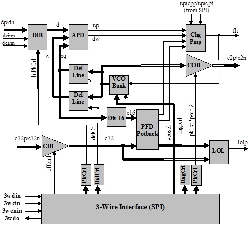
Fig. 1. Functional Block Diagram
ASNT8161-KMF is a half-rate integrated clock recovery (CR) circuit. The IC shown in Fig. 1 covers a wide range of input data rates (fbit) by utilizing its six on-chip VCOs (voltage-controlled oscillators). To reduce the physical number of control inputs to the chip, a shift register with a 3-wire input interface (SPI) has been included on chip. The SPI block provides all the digital controls for the chip. It also provides digital controls for digital-to-analog converters (DACs) that handle internal analog DC voltage adjustments.
Selection of the desired working data rate of the CR is accomplished through the digital control vcosel (see Table 1). An external low speed system clock c32p/c32n running at 1/32 the frequency of the active VCO must be applied to the low-speed clock input buffer (CLK IB). The main function of the chip is to recover from an NRZ or PAM4 input data signal dp/dn with a bit rate of fbit accepted by CML buffer (Data IB) a half-rate clock c2p/c2n that is delivered to the output by the CML clock output buffer (COB). For example, a 28GHz clock signal will be generated from a 56Gb/s input data signal. The digital byte delCrl of SPI is used to properly set phases of the internal clock signals.
Data IB can operate with either differential or single-ended input signals. The buffer can provide a controlled peaking for the input signal (through the SPI). The buffer also includes tuning pins dcinp/dcinn for DC offset of the input signals in case of AC termination. When the buffer is operating with a DC-terminated single ended input signal, a correct threshold voltage should be applied to the unused input pin. All CML I/Os provide on chip 50Ohms termination to vcc and may be used differentially, AC/DC coupled, single-ended, or in any combination (see POWER SUPPLY CONFIGURATION within the Product Datasheet). A loss of lock CMOS alarm signal lolp is generated by the CR to indicate its locking state. An off chip passive filter is required by the CR, and should be connected to pin ftr (see Core section). The clock recovery circuit is characterized for operation from 0°C to 125°C of junction temperature. The package temperature resistance is 15°C /W.