
Product Details
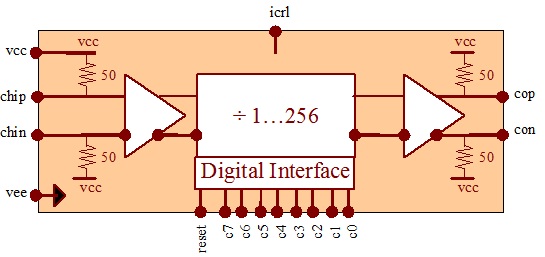
Fig. 1 Functional Block Diagram
ASNT8110-PQB is a high-speed programmable integer clock divider with static or dynamic adjustment of the division ratio through a standard 8-bit parallel LVTTL/CMOS interface and optional external reset (active-high CMOS/LVTTL signal). The functional block diagram of the device is shown in Fig. 1.
The divider accepts an input clock signal chip/chin with a speed from DC to the maximum specified frequency and provides a clean 50% duty cycle output divided clock signal cop/con in any operational mode. The divider allows for both static and dynamic adjustment of the division ratio from 1 to 256 with a step of 1. In the static mode, the binary code on the control inputs c0-c7 defines the value of the ratio from 1 to 255, where c7 is the most significant bit. All “0”s (“low” state) define the division by 256. Following any change of the control signals in the dynamic mode, the divider switches to idle after (64…128) periods of the high-speed system clock plus an additional 1.6ns delay, and returns back to normal operation with the new division ratio after an additional delay equal to 192 periods of the high-speed system clock.
The device automatically resets itself after the initial power-up and any change of the division control signals. When the optional external reset signal reset is set to “high”, the divider switches to idle (static “0” output) after a 0.7ns delay as shown in the timing diagram in Fig. 2 within the part’s datasheet. When reset returns to “low”, the divider switches back to normal operation after (64…128) periods of the high-speed system clock plus an additional 1.6ns of delay. The minimum allowed reset pulse must not be shorter than 64 periods of the high-speed system clock.
The part’s I/O’s support the CML logic interface with on chip 50Ω termination to vcc and may be used differentially, AC/DC coupled, single-ended, or in any combination. In the DC-coupling mode, the input signal’s common mode voltage should comply with the specifications shown in the electrical characteristics section within the part’s datasheet. In the AC-couping mode, the input termination provides the required common mode voltage automatically. The differential DC signaling mode is recommended for optimal performance.