
Product Details
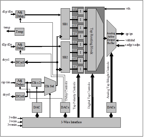
Fig. 1 Functional Block Diagram
The ASNT6102-KMF SiGe IC shown in Fig. 1 is a PAM4 encoder with built-in 4-tap pre-emphasis in each of the two input data channels. Each of the two differential input NRZ data streams is processed by a 4-tap shift register. Both 4-bit shift registers are activated by the same internal high-speed clock signal. As a result, the two registers provide 8 delayed copies of the two data input signals d1p/d1n (MSB Signal) and d2p/d2n (LSB Signal). These copies are combined together with certain user-controlled weights and polarities and are added together. The resulting differential analog data output data is sent to output port qp/qn. In order to get a PAM4 signal at the output the combined tap weight of the MSB signal should be two times greater than the combined tap weight of the LSB signal. For more information see Sampling Block and Taps and Data Output Buffer.
All internal analog control signals, with the exception of the eye crossing adjustment signal xadjp/xadjn, are generated with 8-bit or 12-bit digital-to-analog converter (DAC) blocks. Digital inputs of these DAC blocks are provided by a 3-wire serial interface (SPI) block. All operational modes of the chip are controlled through the SPI block as well. The SPI block is powered by internally generated supply voltage of +1.2V from vee. For more details see 3-Wire Interface Control Block.
The internal clock signal that latches data in the sampling blocks is a copy of the input clock signal cip/cin with either matching or doubled (multiplied-by-2) frequency. In the multiply-by-2 clock mode, the duty cycles of the input and internal clock signals are monitored, and the output duty cycle can be adjusted through a designated control (see Clock Multiplier). For the part’s correct operation, the input data rate in Gbps should be equal to the internal clock frequency in GHz.
Input clock and two data signals can be delayed independently by three control signals to ensure their correct phase relation at the inputs of the shift registers and at the chip outputs (see Input Delay Section).
The part’s I/Os support CML logic interface with on-chip 50Ohm termination to ground. External 50Ohm termination is also required. DC-coupling for data and clock output ports is strongly recommended. The input ports can use DC or AC coupling. Differential connections of input clock and data are strongly recommended. Amplitude and peaking in data output signal can be adjusted. Both single-ended data output signals also have controlled eye crossing points (see Data Output Buffer).
The chip operates from one negative power supply (positive pin connected to external Ground,) and one floating positive power supply (negative pin connected to vee and positive pin v3p5 = 3.5V). It is recommended to keep the relative deviation of v3p5 from Ground within less than ±0.1V.
Additional supply voltage for internal CMOS circuitry is generated inside the chip or may be applied externally to pins v1p2.