Product Details
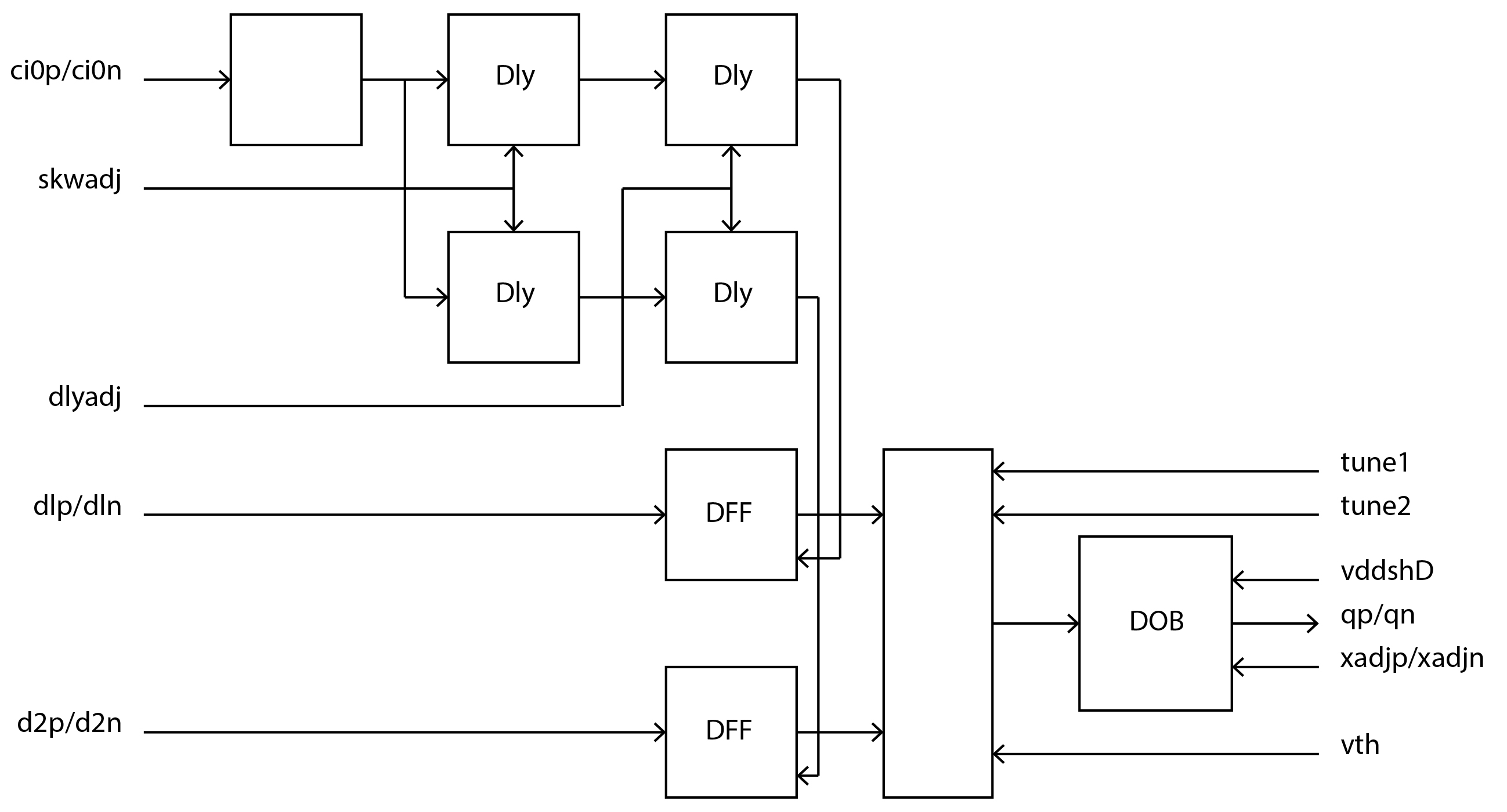
Fig. 1 Functional Block Diagram
This product is now obsolete, and has been superseded by ASNT6103-KMF, which can be found below.
The ASNT6101-KMM SiGe IC shown in Fig. 1 is a single lane PAM4 encoder. It takes two binary input data signals d1p/d1n,and d2p/d2n, retimes them with the input clock ci0p/ci0n, and then combines them into a 4 level output signal (PAM4)qp/qn. The input data rates in Gbps should be equal to the input clock frequency in GHz. The output data symbol rate will be equal to the input data symbol rate, but deliver twice the amount of data due to the multiple levels (i.e. twice the input data bit rate). For example, if the input data and clock are at 20Gb/s, and 20GHz respectively, then the output signal will be running at 40Gb/s-20Gbaud/s.
The input clock ci0p/ci0n is initially split into two identical paths comprising of several delay adjustable stages. Using skwadj, the delays of the two clock paths can be changed with respect to each other where one path’s delay is increased while the other path’s delay is decreased (or opposite). Both of the clock lanes can be delayed by more or less equal amounts using the control pin dlyadj. These two adjustment pins allow for proper alignment of the clock to the two input data signals at the two re-timing internal D-type flip flops DFF.
After the DFFs, the two signals are combined into a PAM4 signal where d1p/d1n is the MSB, and d2p/d2n is the LSB. External pins tune1, and tune2 can be used to separately adjust the amplitudes of the 3 upper signal levels in the PAM4 signal (i.e. independently adjust the weights of the MLB and the LSB). Pin tune1 adjusts the weight of d1p/d1n’scontribution to the PAM4 signal while pin tune2 adjusts the weight of d2p/d2n’s contribution. Pin vth can be used to adjust all 3 upper signals simultaneously, and can be considered the part’s output amplitude control.
Further signal shaping can take place in the data output buffer DOB using control signals vddshD, and xadjp/xadjn. PinvddshD can improve the quality of the output eye by increasing/decreasing under/overshoot. Differential analog control voltage xadjp/xadjn can be utilized to adjust the crossing points of single-ended output eyes. At the default state of xadjp= xadjn = 0V, the crossing points in both direct and inverted eyes should be centered. The crossing points are moving up in the direct eye and down in the inverted eye if xadjp = -xadjn > 0, or in the opposite directions if xadjp = -xadjn < 0.
The part’s I/Os support CML logic interface with on-chip 50Ω termination to ground. External 50Ohm termination is also required, and is usually provided by the adjacent IC or when testing measurement instrumentation is used. DC-coupling for the data output ports is strongly recommended. The input ports can use DC or AC coupling. Differential input clock, and data are strongly recommended.
Evaluation Boards - 1
Application Notes
ASNT6101-KMM Evaluation Board
53 Gb/s - 26.5Gbaud/s PAM4 Signal Generator / Encoder
Application Note
Evaluation Board
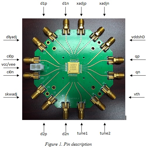
ADSANTEC’s evaluation board (EVB) ASNT21_2 contains 16 edge-mount Emerson female connectors MFG PN: 142-0761-881 SMA, 50Ohm transmission lines to the chip, and includes a MOLEX connector PN: 39-28-1023 to supply power (VCC(GND) - left, VEE - right). Figure 1 shows the EVB with its corresponding pin connections.