Product Details
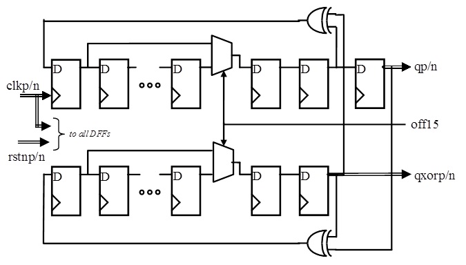
Fig.1 Functional Block Diagram
The ASNT8142-KMC SiGe IC shown in Fig. 1 provides a selectable full 32767-bit or 127-bit long pseudo-random binary sequence (PRBS) signal according to either (x15 + x14 + 1) or (x7 + x6 + 1) polynomial respectively, where xD represents a delay of D clock cycles. This is implemented as a linear feedback shift register (LSFR) in which the outputs of the seventh and sixth flip-flops are combined together by an XOR function and provided as an input to the first flip-flop of the register. The polynomial is selected through the external control signal off15.
The LSFR-based PRBS generator produces binary states, excluding the “all zeros” state that is illegal for the XOR-based configuration. To eliminate this state that locks the LSFR and prevents the PRBS generation, an asynchronous external active-low preset signal (rstnp/rstnn) is implemented in the circuit. When the preset is asserted, LSFR is set to the All-“1” state that is enough for activation of the PRBS generation. When the preset is released, the chip delivers one consecutive bit of the PRBS signal to output pins qp/qn per each rising edge of clock clkp/clkn, starting from the above mentioned state.
An additional copy of the same PRBS signal delayed by XX bits (half of the sequence period) is delivered to pins qxorp/qxorn and can be used to double the frequency of the output signal using an external multiplexer. All I/O stages are back terminated to vcc with on-chip 50Ω resistors and may be used in either DC or AC coupling modes. In the first mode, the input signal’s common mode voltage should comply with the specifications shown in the electrical characteristics section of the part’s datasheet. In the second mode, the input termination provides the required common mode voltage automatically. The differential DC signaling mode is recommended for optimal performance.