
Product Details
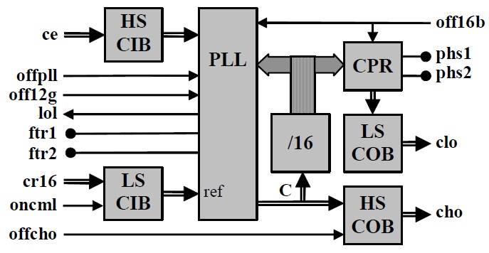
Fig. 1 Functional Block Diagram
ASNT8050-PQB is a clock multiplication unit (CMU) with a dual-range phase-locked loop (PLL) incorporating high-speed voltage-controlled oscillators (VCOs). The part features several control functions shown in Table 1 within the part’s datasheet.
One of the two frequency ranges can be selected by the control signal off12g. In the main operational mode, the IC shown in Fig. 1 accepts a low-speed reference clock cr16p/cr16n with the frequency f/8 or f/16 and converts it into a high-speed output clock cho with the frequency f and the low-speed output clock clo with the corresponding frequency f/8 or f/16. The frequency of the reference and output clocks is defined by the settings of control signal off16b.
The high-speed clock output buffer can be enabled/disabled by the control signal offcho. One of four 90° shifted phases of the low-speed output clock with the frequency f/16 can be selected by control signals phs1 and phs2. This phase selection is not available for the output clock with the frequency f/8.
When operating in the closed-loop mode, the PLL requires an external loop filter connected to pins ftr1 and ftr2. The output signal lol indicates the locked or unlocked state of the PLL. The PLL also supports an open-loop mode of operation with its selected VCO controlled externally by voltages applied to the filter pins ftr1 and ftr2. The chip can operate as a divider of the input high-speed clock cep/cen if the PLL is disabled by the control signal offpll. The division ratio of 8 or 16 can be selected by the control signal off16b. The part makes use of a single +3.3V power supply, and is characterized for operation from -25°C to 125°C of junction temperature.