Product Details
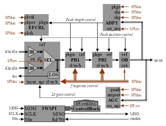
Fig. 1 Functional Block Diagram
The ASNT6750 is an adjustable continuous-time linear equalizer (CTLE) with a possibility of manual or automatic adaptation to a user-defined frequency response. One of two input signals d1p/d1n or d2p/d2n, selected by the on_d2 control switch, passes through an equalization data path that consists of four linear current-switching stages. The AC response of the data path can have a variable peak at frequencies from 13GHz to 20GHz. In the manual mode (switches on_agc and on_aeq are “Low”), the channel’s gain can be adjusted by the controls pkgn and gn. The peak’s value, position, and shape can be adjusted by controls zl, zm, zh, zob, pkval, pkpos, and pksh. In the automatic mode, the channel needs an initial calibration using manual controls (switches on_agc and on_aeq are “Low”). The peak frequency position and its minimum/maximum values are defined during the calibration. After that (switches on_agc and on_aeq are “High”) it automatically adjusts to a user-defined output amplitude set by control ampset and to an optimal peak value that corresponds to a user-defined non-distorted output signal spectrum density. The part’s I/Os support CML-type differential interface with on-chip 50Ohms termination to vcc at the inputs and on-chip 50Ohms termination to vcc at the output. Matching external terminations are also required. Critical internal voltages can be controlled through DC test points (dctpx) that need capacitive decoupling to vee on PCBs.
The part operates with a positive supply vcc = +3.3V for the main data path, and additional positive supplies v4p3 = +4.3V for the AC control circuitry and v3p7 = +3.7V for the input buffer stage. The negative supply rail vee should be connected to external ground.