Product Details
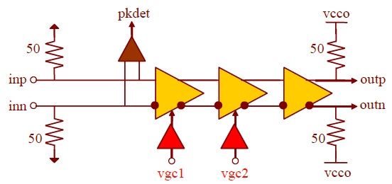
Fig. 1 Functional Block Diagram
The temperature-stable linear amplifier ASNT6141-KMC IC shown in Fig. 1 has been fabricated in the SiGe technology and provides low-jitter broadband variable signal amplification between its input inp/inn and output outp/outn signal ports and is intended for use in high-speed communication systems. The gain adjustment is performed through two independent external control ports vgc1 and vgc2.
The part’s I/Os support the CML-type interface with on chip 50Ω termination to vcc and may be used differentially, AC/DC coupled, single-ended, or in any combination. In the DC-coupling mode, the input signal’s common mode voltage should comply with specifications shown in the electrical characteristics table within the part’s datasheet. In the AC-coupling mode, the input termination provides the required common mode voltage automatically. The on-chip peak detector delivers a single-ended output voltage pkdet proportional to the input signal’s amplitude. For optional output common-mode voltage adjustment, the output termination resistors can be connected to a separate positive power supply voltage vcco which may be different from vcc. The differential DC signaling mode is recommended for optimal performance.