Product Details
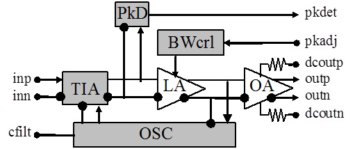
Fig. 1 Functional Block Diagram
The ASNT6121-BD IC is a temperature stable SiGe transimpedance amplifier that provides low-jitter broadband conversion of current signals at its input port inp into differential voltage signals at the output ports outp/outn. The part is a serial combination of transimpedance (TIA), limiting (LA), and linearized output (OA) amplification stages. The part operates as a linear amplifier for low input currents and moves to limiting mode above the specified maximum Non-Limiting Current Swing (see ELECTRICAL CHARACTERISTICS). The input signal should be single-ended with the current flowing into the inp pin. It is recommended to decouple the inn pin to ground with a 10nF capacitor. The part incorporates a control block (BWcrl) with an external port pkadj for adjustment of the total bandwidth or peaking of the amplifier, as well as an automatic DC offset control (OSC) that effectively eliminates any difference between the common-mode voltages of direct and inverted output signals. The offset compensation function requires utilization of an external 100nF capacitor attached to the cfilt pad. The output common mode voltages on output pins outp/outn can be adjusted using analog ports dcoutp/dcoutn respectively.
The on-chip peak detector (PkD) provides an output signal pkdet proportional to the value of the input signal. The on-chip temperature sensor is a diode with its anode connected to the dtemp port. The part’s outputs support a CML-type interface with on-chip 50Ohm termination and may be used as a differential or single-ended connection with AC or DC-coupling (see also POWER SUPPLY CONFIGURATION). The input and output termination resistors in both channels are respectively connected to separate internal positive supply plains vcca and vccd. The input and output negative supply nets are also created as separate metal plains veea and veed, which are partly shorted through the common substrate.