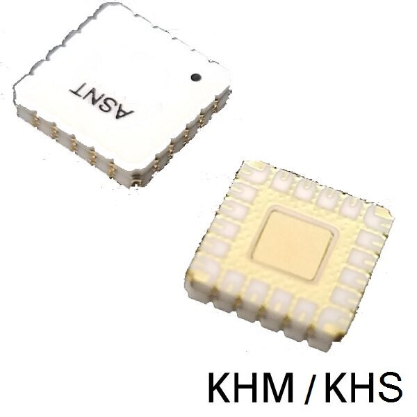
Product Details
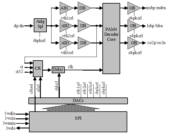
Fig. 1. Functional Block Diagram
The ASNT6106 PAM4 with a built-in clock recovery circuit allows a high-speed differential PAM4 input data signal dp/dn to be processed by an analog splitter (Anlg Spl) with peaking adjustment capability. The three versions of the input signal are delivered to three analog buffers (AB1, AB2, and AB3) with adjustable differential thresholds. The resulting signals are converted into binary pulses by the three limiting digital buffers (DBs) and sent to a PAM4 Decoder Core. The output of the second DB is also sent to the clock recovery block (CR) that requires a low-speed reference clock applied to the port ci32 for correct operation. The part can also operate without clock recovery with an external high-speed clock applied to the port ci.
The three differential binary data streams in PAM4 Decoder Core are first retimed using a full-rate clock provided by CR, and then decoded into two NRZ data signals. The phase of the retiming clock can be adjusted in respect to the data streams by an adjustable delay line (Delay). The decoded most-significant and least-significant NRZ signals are retimed again and delivered to the corresponding output ports msbp/msbn and lsbp/lsbn through Output Buffers (OBs). The retiming clock signal is divided by 2 and delivered to the output port co2p/co2n through a matching OB to ensure phase matching between the output data and clock signals. To reduce the physical number of pins, a 3-wire control interface (SPI) has been included in the chip. The SPI block provides all digital controls for the chip and also controls digital-to-analog converters (DACs) that handle internal analog DC voltage adjustments. Refer to the product datasheet for further information.

