
Product Details
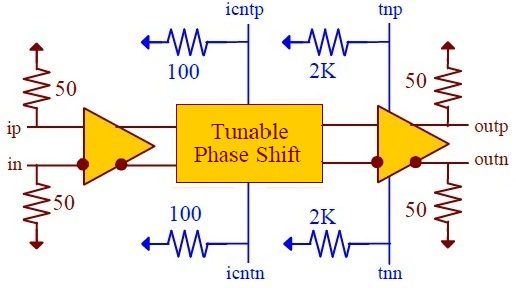
Fig. 1 Functional Block Diagram
ASNT5173-PQC is a data / clock variable delay line fabricated in SiGe technology. The IC shown in Fig. 1 provides an adjustable delay of its differential output signal outp/outn in relation to its broadband input signal ip/in. The delay is controlled through a wide-band differential tuning port icntp/icntn.
The part’s I/O’s support the CML logic interface with on chip 50Ω termination to vcc and may be used differentially, AC/DC coupled, single-ended, or in any combination. In the DC-coupling mode, the input signal’s common mode voltage should comply with the specifications shown in the electrical characteristics section within the part’s datasheet. In the AC-coupling mode, the input termination provides the required common mode voltage automatically. The differential DC signaling mode is recommended for optimal performance.