Product Details
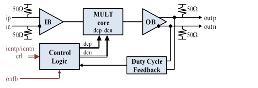
Fig. 1 Functional Block Diagram
The temperature stable ASNT5144-KMC SiGe IC provides broadband frequency multiplication, and is intended for use in high-speed measurement / test equipment. The IC shown in Fig. 1 can receive a high-speed clock input signal ip/in and deliver a high-speed double frequency clock output signal outp/outn. There are two duty cycle correction feedback loops. The first loop adjusts the duty cycle of the input signal, and the second loop controls the final output signal duty cycle. When both feedback loops are activated, the output clock’s duty cycle is automatically kept at about 50%. To ensure correct operation of the feedback block within a wide range of frequencies, the optional control port crl can be set to vee/vcc/nc according to Table 2 within the product datasheet. Activation of the loops is controlled via the onfb control port as shown in Table 1 within the product datasheet.
The part’s I/O’s support the CML logic interface with on chip 50Ω termination to vcc and may be used differentially, AC/DC coupled, single-ended, or in any combination. In the DC-coupling mode, the input signal’s common mode voltage should comply with the specifications shown in the electrical characteristics section within the part’s datasheet. In the AC-coupling mode, the input termination provides the required common mode voltage automatically. The differential DC signaling mode is recommended for optimal performance.