Product Details

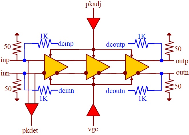
Fig. 1 Functional Block Diagram
The temperature stable ASNT5136-BD SiGe IC provides low jitter broadband variable signal amplification between its input and output signal ports and is intended for use in high-speed communication systems. The circuit shown in Fig. 1 accepts an analog signal at its input differential port inp/inn and delivers a voltage-limited output signal at the output differential port outp/outn. The common-mode voltage levels of input and output signals can be adjusted using analog control inputs dcinp/dcinn and dcoutp/dcoutn respectively. The total gain can be externally adjusted through the gain control port vgc. The output signal’s peaking can be controlled through the port pkadj. The input amplitude can be monitored using the analog output voltage pkdet.
The part’s I/Os support the CML logic interface with on chip 50Ω termination to vcc and may be used differentially, AC/DC coupled, single-ended, or in any combination. In the DC-coupling mode, the input signal’s common mode voltage should comply with the specifications shown in the electrical characteristics section within the part’s datasheet. In the AC-coupling mode, the input termination provides the required common mode voltage automatically. The differential DC signaling mode is recommended for optimal performance.
