Product Details

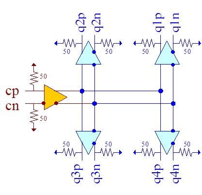
Fig.1 Functional Block Diagram
This part is scheduled for EOL after Q2 of 2024, and is being superseded by the ASNT5723-PQC which can be viewed here:
The ASNT5023-PQC can be used as a Fanout Buffer, Clock Buffer, Clock Distributor, or Clock Splitter which operates from DC to 28Gbps and from DC to 17GHz. The component shown in Fig. 1 provides four phase-matched copies of the broadband input signal cp/cn to four high-speed differential outputs q1p/q1n, q2p/q2n, q3p/q3n, q4p/q4n.
Using it as a Fanout Buffer will allow you to create numerous copies of input signal at their output, which you can in turn divide amongst multiple loads all the while acquiring fast rise/fall time and low jitter.
The part’s I/Os support the CML logic interface with on chip 50Ω termination to positive power supply rail and may be used differentially, AC/DC coupled, single-ended, or in any combination. In the DC-coupling mode, the input signal should have a specific common mode voltage. In the AC-coupling mode, the input termination provides the required common mode voltage automatically. Optimal performance is achieved with differential DC signaling mode.
