Product Details

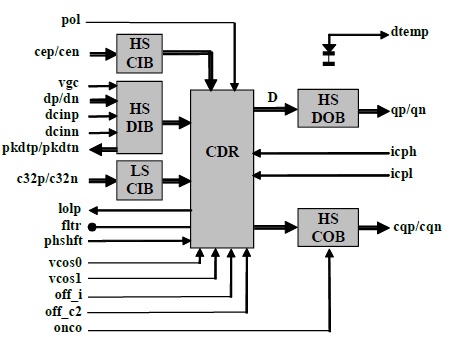
Fig. 1. Functional Block Diagram
This product is approaching End of Life and will soon no longer be available.
ASNT2116-KMF is a 1:1 full-rate clock and data recovery unit (CDR). The main function of the IC shown in Fig. 1 is to recover a full-rate clock signal C and a retimed data signal D from an RZ or NRZ input data signal dp/dn with a bit rate of fbit accepted by a CML input data buffer HS DIB. The IC can function either in CDR mode covering a wide range of input data rates by utilizing its three on-chip VCOs (voltage-controlled oscillators), or in broadband digital mode. Selection of the desired operational mode and the CDR input data rate is accomplished through pins vcos0 and vcos1 (see Table 1). An external low speed reference clock c32p/c32n running at 1/32 of the frequency of the active VCO must be applied to a low-speed LVDS clock input buffer LS CIB in the CDR mode. An external full-rate clock cep/cen must be applied to a high speed CML clock input buffer HS CIB in the digital mode.
The CDR includes two control loops for latching the correct frequency and phase states and requires a single external loop filter connected to pin fltr. The gains of the loops can be tuned independently using control signals icph and icpl. The phase of the clock recovered by the CDR can be adjusted using an external control voltage phshft. This helps achieve the lowest system bit error rate (BER) through selecting the optimal input data sampling time. An internal control circuit generates an alarm signal lolp that indicates the frequency locking state of the CDR.
The data input buffer HS DIB can operate with either differential or single-ended input signals dp/dn. It includes tuning pins dcinp/dcinn for DC offset of the input signals in case of AC termination. When the buffer is operating with a DC-terminated single-ended input signal, a correct threshold voltage should be applied to the unused input pin. A peak detector is also included to provide means of demodulating AM components carried by the input data with a frequency up to a few hundredKHz. The peak detector’s output signal is delivered to a differential port pkdtp/pkdtn.
Depending on the state of control signal off_c2, either a full-rate or a half-rate recovered clock is delivered to outputs cqp/cqn by CML output buffer HS COB. The clock polarity can be inverted using another control signal off_i. The buffer HS COB can be enabled or disabled using control signal onco. The retimed data is delivered to outputs qp/qn by CML output buffer HS DOB. It has a tight phase alignment to output clock cqp/cqn. All CML I/Os provide on chip 50Ω termination to vcc and may be used differentially, AC/DC coupled, single-ended, or in any combination. The LVDS input buffer should be used in accordance with the standard (see LS CIB). The internal temperature can be monitored by a diode’s current running into pin dtemp.
