
Product Details
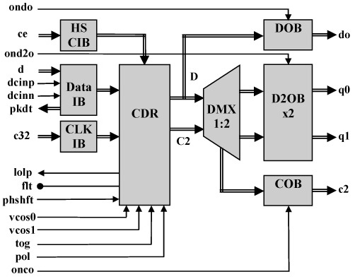
Fig. 1. Functional Block Diagram
ASNT2112-KMF is a 1:2 demultiplexer (DMUX) with full-rate integrated clock and data recovery (CDR). It can function in CDR mode covering a wide range of input data rates (fbit) by utilizing its three on-chip VCOs (voltage-controlled oscillators), or in a broadband digital mode. Selection of the desired working data rate and mode is accomplished through pins “vcos0” and “vcos1”. An external low speed system clock “c32p/n” running at 1/32 the frequency of the active VCO must be applied to the low-speed LVDS clock input buffer (CLK IB) in CDR mode. An external full-rate clock “cep/n” must be applied to the high speed CML clock input buffer (HS CIB) for digital operation.
The main function of ASNT2112-KMF is to convert RZ or NRZ input data signal “dp/n” with a bit rate of fbit accepted by CML buffer “Data IB” into 2 parallel NRZ data signals “q0p/n” and “q1p/n” running at bit rates of fbit/2 and delivered to the outputs by CML data output buffers (D2OBx2). The clock and data are recovered from the input data stream by CDR. The phase of the clock recovered by CDR can be adjusted externally through pin “phshft” to locate the optimum data sampling point to achieve the lowest system bit error rate (BER). A full rate retimed NRZ data output signal “dop/n” is also available through the CML data output buffer (DOB) allowing the part to be used as a 1:1 CDR. Half rate clock “c2p/n” delivered through the CML clock output buffer (COB) has tight phase alignment to demultiplexed data output signals “q0p/n” and “q1p/n”. It operates on a single +3.3V or -3.3V power supply and is characterized for operation from 0°C to 125°C of junction temperature.