Product Details

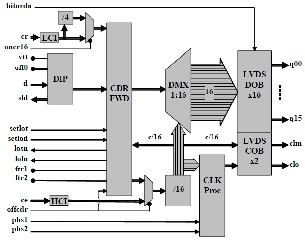
Fig. 1. Functional Block Diagram
ASNT2017-PQA is a user-programmable 14Gbps 1:16 deserializer (DMUX) with a full-rate integrated clock and data recovery unit (CDR) that incorporates a frequency window detector (FWD). The main function of the chip shown in Fig. 1 is to demultiplex a serial input data signal d running at a bit rate of fbit into 16-bit wide parallel data words q00-q15 running at a bit rate of fbit/16. The DMUX can operate in one of two main modes: CDR mode that utilizes on-chip full-rate VCO with a central frequency of fbit, or broadband digital mode that requires application of an external full-rate clock ce with the same frequency to the inputs of a high speed CML clock input buffer (HS CIB). Selection of the operational mode is made through control pin offcdr.
The high sensitivity CDR FWD block incorporates phase and frequency acquisition loops to ensure accurate recovery of clock and data for an NRZ input data stream. For the correct operation of the block, off-chip passive filter components should be connected to pins ftr1 and ftr2. CDR FWD also requires an external reference clock running at 1/16 or 1/64 the VCO’s frequency to be applied to the input cr. The acceptable frequency of the reference clock is defined by the oncr16 control signal. If the 1/16 mode is selected, the input clock with frequency of fbit/16 is applied to CDR FWD after an additional divider by 4 (/4). The reference clock input buffer supports LVDS or CML interfaces as defined by the oncml control signal. The recovered clock is used for sampling the input data bits before they are demultiplexed and is also sent to the internal divider (/16). CDR FWD also provides active-low alarm indicators for loss of input signal (losn) and loss of lock (loln).
The high-speed CML data and clock input buffers provide on-chip 50Ohm termination and are designed to be driven by devices with 50Ohm source impedance. The data input buffer sets its termination voltage internally, but the vtt pin can be used to externally adjust it if desired. Pin off0 control the offset voltage between data inputs dp and dn allowing the user to change the slicing or threshold level at the serial data input. A peak detector is incorporated in Data IB to monitor the amplitude of the incoming data stream with its output made available through differential pins sld.
The reconstructed serial input data is latched into the demultiplexer (DMX1:16) and is subsequently deserialized and delivered to the demultiplexer’s output as 16-bit wide low-speed parallel words. Sixteen proprietary low-power LVDS output data buffers (LVDS DOBx16) are used to deliver the 16 data output signals q00-q15, while a similar dual LVDS clock output buffer (LVDS COBx2) outputs the two copies clm and clo of the low-speed clock signal. The buffers satisfy all the requirements of the IEEE Std. 1596.3-1996 and ANSI/TIA/EIA-644-1995 standards. The phase of the clo clock signal can be selected with a 90° increment by utilizing control pins phs1 and phs2.
Utilizing control pin bitordn, the deserializer can designate either q00 or q15 as the MSB (first input serial bit), thus simplifying the interface between the demultiplexer chip and a following ASIC. The chip uses a single +3.3V power supply and is characterized for operation from −25°C to 125°C of junction temperature.
