
Product Details
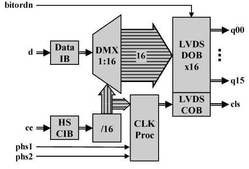
Fig. 1. Functional Block Diagram
ASNT2011-PQA is a low power and high-speed digital 1 to 16 demultiplexer / deserializer IC. The part can function seamlessly over input data rates (fbit) ranging from DC to 17Gbps. The main function of ASNT2011-KMA is to demultiplex a serial input data channel d running at a bit rate of fbit into 16 parallel data channels q00-q15 running at a bit rate of fbit/16. The high sensitivity data input buffer (Data IB) ensures accurate operation at low input data signal amplitudes. It provides on-chip 50Ω termination to vcc and is designed to be driven by devices with 50Ω source impedance.
During normal operation, the received serial input data is latched into a tree-type demultiplexer DMX1:16 and subsequently deserialized and delivered to the demultiplexer’s output as 16-bit wide low-speed parallel words. The output MSB corresponds to q00 when bitordn=0 (default), or to q15 when bitordn=1.
A full rate clock must be provided by an external source ce to the high-speed clock input buffer HS CIB where it is routed to the internal divider-by-16 (/16). The divider provides signaling for DMX1:16 and produces a full rate clock divided-by-16 C16 for the low speed LVDS compliant clock output buffer LVDS COB. The phase of cls can be modified by 90° increments by utilizing pins phs1 and phs2 and the clock processing block CLK Proc.
Sixteen proprietary low-power LVDS output data buffers LVDS DOBx16 are used to deliver the 16 data output signals q00-q15 while a similar LVDS clock output buffer LVDS COB outputs the low-speed clock signal cls. The deserializer uses a single +3.3Vpower supply and is characterized for operation from −25°C to 125°C of junction temperature.