Product Details

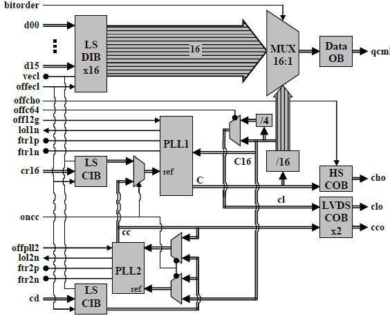
Fig. 1. Functional Block Diagram
ASNT1016-PQA is a low power and high-speed 16 to 1 multiplexer (MUX) with an internal clock multiplier unit (CMU). The MUX can function at data rates (fbit) between 9.8Gbps to 12.5Gbps by utilizing its multiple on-chip full-rate VCOs.
The main function of ASNT1016 is to multiplex 16 parallel data channels running at a bit rate of fbit/16 into a high speed serial bit stream running at fbit. It provides a high-speed output data channel for point-to-point data transmission over a controlled impedance media of 50Ω. The transmission media can be a printed circuit board or copper coaxial cables. The functional distance of the data transfer is dependent upon the attenuation characteristics of the transportation media and the degree of noise coupling to the signaling environment.
During normal operation, the serializer’s low-speed input buffer (LS DIBx16) accepts external 16-bit wide parallel data words “d00”-“d15” through 16 differential inputs with reconfigurable LVDS/CML/ECL interfaces and delivers them to the multiplexers core (MUX16:1) for serialization. The desired input data interface is selected by the CMOS input control signal “offecl” while the proper input termination voltage is provided by “vecl”. By utilizing pin “bitorder”, the serializer can designate either “d00” or “d15” as the MSB thus simplifying the interface between ASNT1016 and a proceeding ASIC.
MUX16:1 serializes the data words with multiple divided down clock signals that are generated from the full rate clock “C” by the internal divider (/16). The divider also produces a full rate clock divided-by-16 signal “C16” for use by both phase locked loops. “C” is synthesized by the main phase-locked loop (PLL1) that references either an external system level clock “cr16” delivered by one of the low speed clock input buffers (LS CIB) or the internal clock “cc” that is generated by the secondary phase locked loop (PLL2) in concert with a different external low speed clock “cd”. Both “cr16” and “cd” must be 1/16 the frequency of the active full rate VCO in PLL1. PLL1 contains 2 full rate VCOs to cover the 9.8-12.5GHz range, which are selected utilizing the “off12g” control pin.
ASNT1016 offers 3 different kinds of clocking modes. In the default state, PLL2 is turned off through pin “offpll2” and PLL1 is locked to the “clean” system clock “cr16”. In the forward clocking mode (“offpll2”=0 & “oncc”=0), an active PLL2 is locked to the “dirty” external clock “cd” provided by the preceding ASIC in parallel with the input data and generates a “clean” reference clock “cc” for PLL1. The “clean” system clock “cr16” is not needed since PLL2 provides “clock cleaning” functionality.
In the counter clocking mode (“offpll2”=0 & “oncc”=1), PLL2 is used to ensure a robust interface between the driving ASIC and ASNT1016. PLL1 is locked to the “clean” system clock “cr16”, while PLL2 is locked to “C16”, which is generated by PLL1 and /16. The low speed output clock from PLL2 “cco” controls the output stage of the preceding ASIC and initiates the transmission of its parallel data and respective clock “cd” across the parallel bus to the inputs of ASNT1016-PQA.
The serialized words are transmitted as 2-level signals “qcml” by a differential CML output buffer (Data OB). A full-rate clock “cho” is transmitted by a similar CML buffer (HS COB) in parallel with the high-speed data. The clock and data outputs are well phase matched to each other resulting in very little relative skew over the operating temperature range of the device. HS COB may be disabled to save power by means of the 2-state CMOS “offcho” signal. Both output stages are back terminated with on-chip 50Ω resistors.
ASNT1016 also provides a differential low speed output clock derived from PLL1 though a LVDS clock output buffer (LVDS COB). This LVDS output signal “clo” may be configured for either “C16” or full rate clock divided-by-64 “C64” operation through pin “offc64”.
Both PLL1 and PLL2 generate loss of lock signal alarms “lol1n” and “lol2n”. Off chip capacitors are required for both PLLs and are connected through pins “ftr1p/n” and “ftr2p/n”. The serializer uses a single +3.3V power supply and is characterized for operation from −25°C to 125°C of junction temperature.


