Product Details
ASNT6101-KMM-Evaluation Board
53Gb/s – 26.5Gbaud/s PAM4 Signal Generator / Encoder
Overview
The ASNT6101-KMM is a single lane PAM4 encoder. It takes two binary input data signals d1p/d1n, and d2p/d2n, retimes them with the input clock ci0p/ci0n, and then combines them into a 4-level output signal (PAM4) qp/qn. The input data rates in Gbps should be equal to the input clock frequency in GHz. The output data symbol rate will be equal to the input data symbol rate, but delivers twice the amount of data due to the multiple levels (i.e. twice the input data bit rate).
Evaluation board
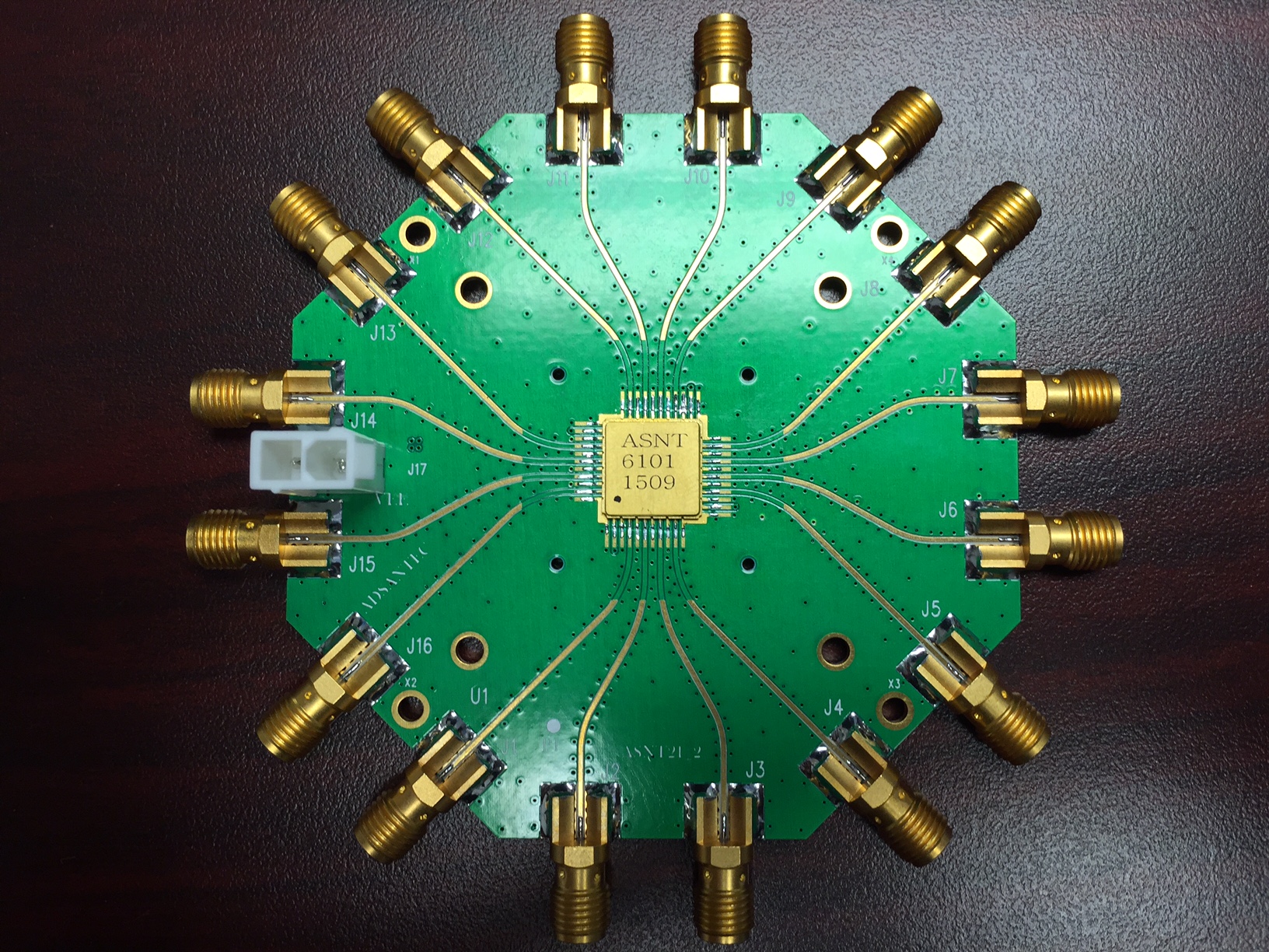
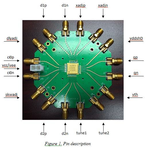
ADSANTEC’s evaluation board (EVB) ASNT21_2 contains 16 edge-mount Emerson female connectors MFG PN: 142-0761-881 SMA, 50Ohm transmission lines to the chip, and includes a MOLEX connector PN: 39-28-1023 to supply power (VCC(GND) – left, VEE – right). Figure 1 shows the EVB with its corresponding pin connections.
Operation
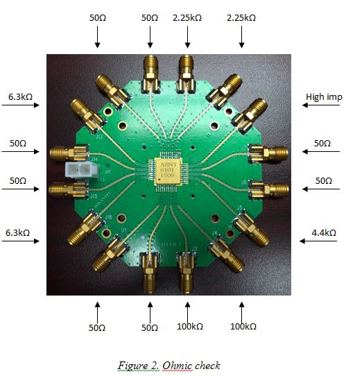
- Measure the resistance of all connector pins in reference to VCC (GND), including the power supply VEE (high impedance). Figure 2 shows the approximate corresponding resistance values for all the board’s edge connectors.
- Set a negative power supply to 0V, while placing its current limit at 400mA. Ramp the supply slowly up to -3.3V. The board should draw approximately 350mA.
- Apply the following voltages to these pins:
a. skwadj -0.8V
b. tune 1 -0.55V
c. tune 2 -0.55V
d. vddshD 0.0V
These values will need to be slightly adjusted to optimize the output signal, so ensure the voltages applied can be altered.
- Apply a single-ended AC coupled or differential DC coupled (preferred) clock signal with amplitude at least 400mV peak-to-peak to ci0p and ci0nn. Terminate any unused input port with 50Ohms.
- Apply single-ended AC coupled or differential DC coupled (preferred) data signals with amplitudes at least 400mV peak-to-peak to d1p/d1n and d2p/d2n. Terminate any unused input port with 50Ohms.
- Connect qp/qn directly to a 50Ohm terminated oscilloscope. Terminate any unused output port with 50Ohms.
- All other connectors on the board can be left unconnected.
- To ensure that the two input data signals are being clocked into the chip correctly (i.e. error free), a good practice to follow is to turn the weight of one of the input signals fully on (the one you are checking) while turning the other one completely off and checking the resulting output signal for errors. For example, to see if d1p/d1n is being clocked in without errors, adjust tune 1 to 0.0V and tune 2 to -2.0V and observe the output signal. If there are errors, then adjust the delay of the input data signal into d1p/d1n appropriately. It’s important to be sure that both input data signals are clocked in correctly. Once this is verified, place tune 1 and tune 2 back to their original voltages as stated in Section 3.
- To optimize the output eye, slightly tune the voltages on the pins listed in Section 3 within the ranges specified in the data sheet.
Note: Input and outputs can be operated differentially, single-ended, AC/DC coupled. The connections described above only represent one way of interfacing to the evaluation board. For more detailed information, please refer to the datasheet.