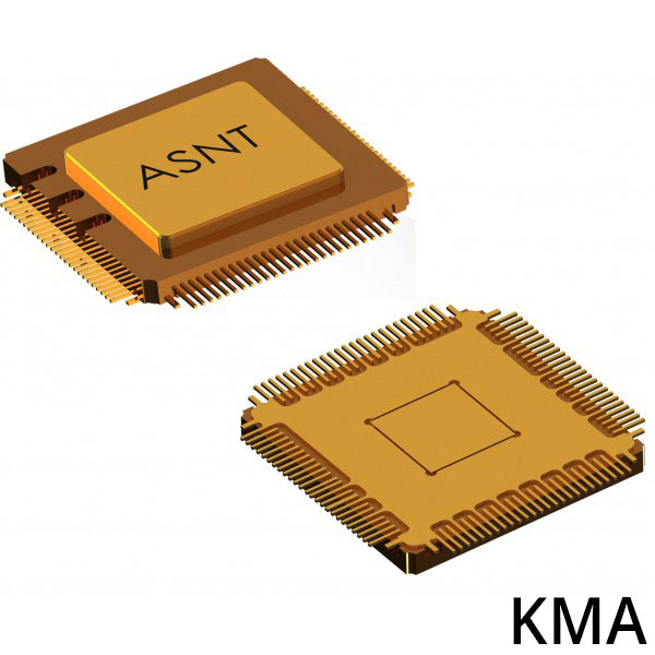
Product Details
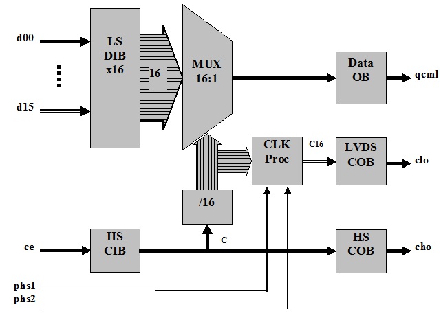
Fig. 1 Functional Block Diagram
ASNT1011-KMA is a low power and high-speed programmable multiplexer (MUX) 16-to-1 (16:1) or 8-to-1 (8:1). The part functions seamlessly over data rates (fbit) ranging from DC to 17Gbps. It’s main function is to multiplex 16 parallel data channels running at a bit rate of fbit/16 into a high speed serial bit stream running at fbit. It provides a high-speed output data channel for point-to-point data transmission over a controlled impedance media of 50Ω. The transmission media can be a printed circuit board or copper coaxial cables. The functional distance of the data transfer is dependent upon the attenuation characteristics of the transportation media and the degree of noise coupling to the signaling environment.
During normal operation, the serializer’s low-speed input buffer (LS DIBx16) accepts external 16-bit wide parallel data words “d00”-“d15” through 16 differential LVDS inputs and delivers them to the multiplexer’s core (MUX16:1) for serialization. A full rate clock must be provided by an external source (“ce”) to the high-speed clock input buffer (HS CIB) where it is routed to the high speed clock output buffer (HS COB) and the internal divider-by-16 (/16). The divider provides signaling for MUX16:1 and produces a full rate clock divided-by-16 “C16” for the low speed LVDS compliant clock output buffer (LVDS COB).The phase of “clo” can be modified by 90° increments by utilizing pins “phs1” and “phs2” and the clock processing block.
During normal operation with M=8 (off16b =”1”), the part operates in a similar way but the serializer’s low-speed input buffer (LS DIBx16) accepts only l 8-bit wide parallel data words d00p/d00n-d07p/d07n through the first eight differential LVDS inputs. In this mode, the divider (/16) also generates a clock divided-by-8 (C8) that is delivered to LVDS COB. The phs1 and phs2 controls are disabled in this operational mode.
The serialized words are transmitted as 2-level signals “qcml” by a differential CML output buffer (Data OB). A full-rate clock is transmitted by HS COB in parallel with the high-speed data. The clock and data outputs are well phase matched to each other resulting in very little relative skew over the operating temperature range of the device. Both output stages are back terminated with on-chip 50Ω resistors. The serializer uses a single +3.3V power supply and is characterized for operation from −25°C to 125°C of junction temperature.
Comparable Parts - 5
ASNT1011-PQA

ASNT1011A-KMA
ASNT1011A-PQA
ASNT1016-PQA