Product Details
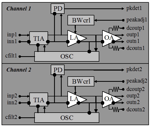
Fig. 1 Functional Block Diagram
TheASNT6123-BD SiGe IC is a two-channel temperature stable SiGe transimpedance amplifier that provides low-jitter broadband linear conversion of current signals at its input ports (inp1/inn1, inp2/inn2) into differential voltage signals at the output ports (outp1/outn1, outp2/outn2). Each channel of the part shown in Fig. 1 is a serial combination of transimpedance (TIA), limiting (LA), and output (OA) amplification stages. The input signal can be either differential or single-ended with the current always flowing into the corresponding pin. In case of one input being single-ended, a certain DC level signal must be applied to the other input. The part incorporates an automatic DC offset control (OSC) that effectively eliminates any difference between the common-mode voltages of direct and inverted output signals. This function requires utilization of external capacitors attached to cfilt1 and cfilt2 pads. The DC common-mode voltage level of each single-ended output can be manually adjusted using the corresponding dcoutp1/dcoutn1 or dcoutp2/dcoutn2 control inputs. The individual amplifier bandwidth can be manually adjusted through changing its peaking characteristics by means of peakadj1 or peakadj2 control signals.