Product Details
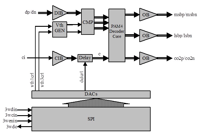
Fig. 1. Functional Block Diagram
The ASNT6104-KMM SiGe IC shown in Fig. 1 is a PAM4 decoder with a built-in clock recovery circuit. The differential PAM4 input data signal dp/dn is processed by the linear input buffer (DIB) and is sent to the Comparator block (CMP), and the Clock Recovery block (CR). Three limiting buffers inside CMP process the 3-level PAM4 signal. One of the buffers processes the input signal differentially. The other two buffers compare single-ended data to their own threshold levels that are produced by the Voltage Threshold Generator block (Vth GEN). The three resulting differential binary data streams are sent to the PAM4 Decoder Core where they are retimed by D-type flip flops (DFFs) with the full-rate clock provided by CR, and delayed by the adjustable delay line block (Delay). The three differential signals are decoded into two differential data streams. The two signals are retimed again, and are sent to the output through Output Buffers (OB). To reduce the physical number of control inputs to the chip, a shift register with a 3-wire input interface (SPI) has been included on chip. The SPI block provides all the digital controls for the chip. It also provides digital controls for digital-to-analog converters (DACs) that handle internal analog DC voltage adjustments.

