Product Details
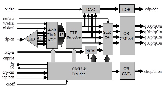
Fig. 1 Functional Block Diagram
The ASNT7123A-KMA is a 4-bit flash analog to digital converter (ADC) featuring a high sampling rate and wide analog front-end bandwidth. The ADC system shown in Fig. 1 includes a linear input buffer (LIB) with tree-type architecture and a CML-type input interface with internal 50Ohm single-ended terminations to vcc. The buffer delivers 15 matching copies of the input analog data signal dp/dn to the 4-bit flash ADC. The ADC creates 15 samples of the input data in thermometer code, which are then converted by a thermometer-to-binary encoder (TTB Encoder) into 4-bit binary words with a data rate f. TheADC thresholds are controlled by signals vrefcrl and vlsbcrl. The encoded data is processed by a scrambler (SCRx4) where it is mixed with a 215-1 PRBS signal provided by an internal PRBS generator (PRBS). The scrambled data is delivered to a 4-bit differential CML output interface (OB CMLx4, pins q00p/q00n, q01p/q01n, q02p/q02n, q03p/q03n). The PRBS generator can be preset to a certain initial state by the differential external signal rstp/rstn, or completely disabled by control signal onprbs. When disabled, the generator allows data to pass unchanged through the scrambler. It is also possible to disable the data by using control signal ondata and pass the PRBS signal to the outputs. An optional digital-to-analog converter (DAC) with an output signal odp/odn can be used to control theADC’s operation. It is enabled by control signal ondac.
All operations are synchronized by the internal clock multiplication unit (CMU) based on aPLL(phase-locked loop) with an integrated divider and an external loop filter connected to pin ftr. The block can operate in two different modes and is controlled by signal ceoff: they can either be clock multiplication (PLL is on, a reference clock is applied to pins crp/crn), or clock division (PLLis off, an external high-speed clock is applied to pins cep/cen). In both modes, the divider generates internal clock signals divided by 2, 4, 8, and 16. The generated divided clocks are sent to different internal blocks. In the second operational mode of the CMU, the divider can be preset by external signal res to allow synchronization of parallel-connected ADCs. A PLL lock control output lol is also provided. The part operates from a single +3.5V power supply. All external control signals are compatible with the 2.5V CMOS interface.