
Product Details
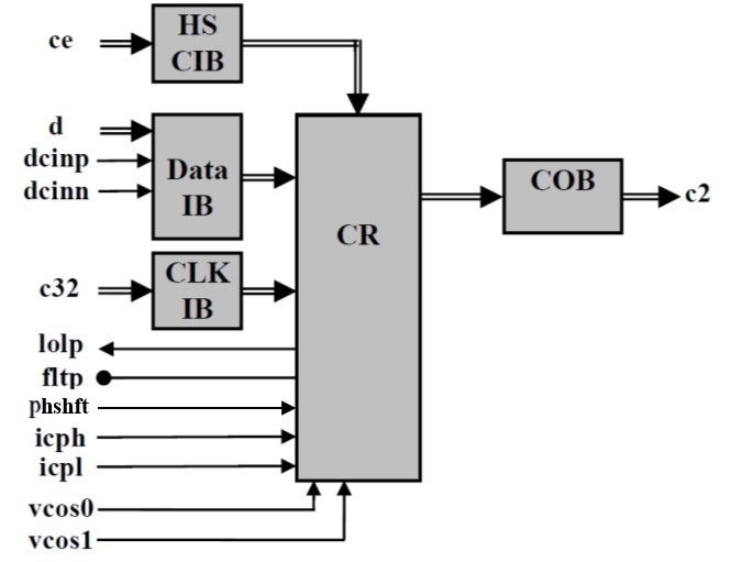
Fig. 1. Functional Block Diagram
ASNT8160C-KMF is a half-rate integrated clock recovery (CR) circuit. The IC shown in Fig. 1 functions in the CR mode covering a wide range of input data rates (fbit) by utilizing its three on-chip VCOs (voltage-controlled oscillators). Selection of the desired working data rate and mode is accomplished through pins vcos0 and vcos1 (see Table 1). An external low speed system clock c32p/c32n running at 1/32 the frequency of the activeVCO must be applied to the low-speed LVDS clock input buffer (CLK IB) for the IC to work properly. The main function of the chip is to recover from an NRZ input data signal dp/dn with a bit rate of fbit accepted by CML buffer (Data IB) a half-rate clock c2p/c2n that is delivered to the output by the CML clock output buffer (COB). For example, a 30GHz clock signal will be generated from a 60Gb/s input data signal.
Data IB can operate with either differential or single-ended input signals. It includes tuning pins dcinp/dcinn for DC offset of the input signals in case of AC termination. When the buffer is operating with a DC-terminated single ended input signal, a correct threshold voltage should be applied to the unused input pin. All CML I/Os provide on chip 50Ω termination to vcc and may be used differentially, AC/DC coupled, single-ended, or in any combination. A loss of lock CMOS alarm signal lolp is generated by the CR to indicate its locking state. An off chip passive filter is required by the CR, and should be connected to pin ftr (see CR section). The clock recovery circuit is characterized for operation from 0°C to 125°C of junction temperature. The package temperature resistance is 15°C /W.