
Product Details
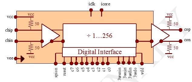
Fig. 1 Functional Block Diagram
ASNT8111A-PQB is a high-speed programmable Clock Divider, Frequency Divider with dynamic adjustment of the division ratio. An optional external active-high CMOS/LVTTL reset signal is also provided. The functional block diagram of the device is shown in Fig. 1.
The component show in Fig. 1 accepts an input clock signal chip/chin with a speed from DC to the maximum specified frequency and provides a clean 50% duty cycle output divided clock signal cop/con. The clock divider allows for dynamic adjustment of the division ratio from 1 to 256 with a step of 1 through either 8-bit parallel interface or 3-wire SPI. An optional external active-high reset signal is also provided.
The part’s I/Os support the CML logic interface with on chip 50Ω termination to positive power supply rail and may be used differentially, AC/DC coupled, single-ended, or in any combination. In the DC-coupling mode, the input signal should have a specific common mode voltage. In the AC-coupling mode, the input termination provides the required common mode voltage automatically. Optimal performance is achieved with differential DC signaling mode.
In the serial mode, the 1-byte division coefficient code is supplied through the 3-wire interface with MSB first as shown in Fig. 2. Input data 3wdin are sampled at rising edges of SPI clock 3wcin and internal division coefficient value will be updated at a rising edge of the 3wenin signal. The device automatically resets itself after the initial power-up and any change of the division control signals. When the optional external reset signal reset is set to “high”, the divider switches to idle (static “0” output) after a 0.7ns delay as shown in the timing diagram in Fig. 3. When reset returns to “low”, the divider switches back to normal operation after (64…128) periods of the high-speed system clock plus an additional 1.6ns of delay. The minimum allowed reset pulse must be longer than 64 periods of the high-speed system clock.