Product Details

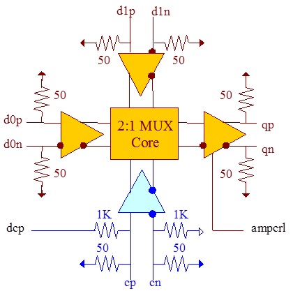
Fig. 1 Functional Block Diagram
The ASNT5650 SiGe IC can be utilized as either a high isolation selector switch or a high speed 2:1 serializer and is intended for use in high-speed measurement / test equipment.
When employed as a selector switch, the IC can route one of its differential data input signals d0p/d0n or d1p/d1n to its differential output qp/qn while effectively blocking the other data input. Selection of a specific data input is achieved through appropriate external DC biasing of the selector signal inputs cp/cn.
As a 2:1 serializer, the IC can receive high speed input data signals into d0p/d0n and d1p/d1n and effectively multiplex them into a double frequency rate NRZ output data signal by using a high speed input clock signal on its selector signal inputs cp/cn. The signals should be aligned as shown in Fig. 2. To ensure both maximum timing margins and low output signal jitter, limit the amount of jitter on the input signals (D0, D1, and C) to only a few picoseconds. The common-mode voltage levels of the input clock signals can be adjusted using an external analog control voltage applied to the port dcp. The output data swing is controlled by an external analog control voltage applied to the port ampcrl.
The part’s I/O’s support the CML logic interface with on chip 50Ohm termination to vcc and may be used differentially, AC/DC coupled, single-ended, or in any combination (see also POWER SUPPLY CONFIGURATION). In the DC-coupling mode, the input signal’s common mode voltage should comply with the specifications shown in ELECTRICAL CHARACTERISTICS. In the AC-coupling mode, the input termination provides the required common mode voltage automatically. The differential DC signaling mode is recommended for optimal performance.
