
Product Details
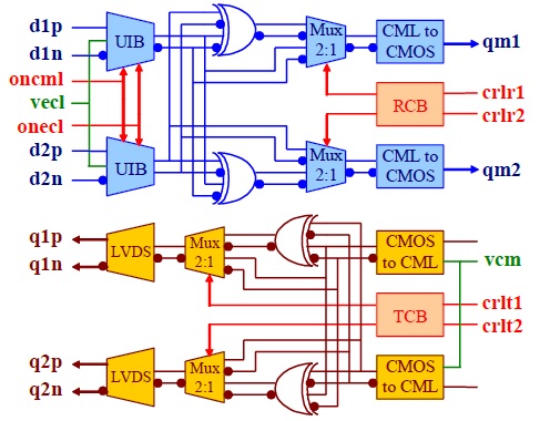
Fig. 1 Functional Block Diagram
ASNT3010-PQB is a bi-directional 4-channel digital interface converter. The part shown in Fig. 1 includes two individual receiver channels with programmable LVDS/CML/ECL differential inputs d1p/d1n, d2p/d2n, and CMOS outputs qm1, qm2; as well as two individual transmitter channels with CMOS inputs dm1, dm2 and LVDS differential outputs q1p/q1n, q2p/q2n.
All channels can be independently enabled or disabled by control signals crlr1, crlr2, crlt1, crlt2. When a receiver channel is disabled, the corresponding CMOS output drivers are set to a high impedance (high-Z) state. The individual receiver or transmitter channels can be combined into a corresponding Space Wire receiver or transmitter with an optional data/strobe (DS) encoding or decoding respectively. The assignment of the data and strobe, or data and clock signals to the individual channels is user-selectable.
Dual transmitter and/or receiver channels can be used for splitting one of the input signals into two exact copies at the two corresponding outputs. The signal at the second output can be inverted using the second input as a selector (a differential DC signal must be applied to the LVDS input). Detailed instructions for using this operational mode are available on request. The converter operates at data rates up to 2Gbps with a nominal power consumption of 115mW from a single +3.3V power supply in a fully activated mode. The device is characterized for operation from −25°C to 125°C of junction temperature.