Product Details
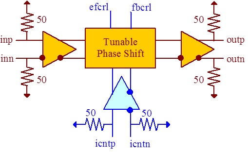
Fig. 1 Functional Block Diagram
ASNT5105A-KMC is a data/clock variable delay line fabricated in SiGe technology. The part provides an adjustable delay of its differential output signal outp/outn in relation to its broadband input signal inp/inn. The delay is controlled through a wide-band differential tuning port icntp/icntn. The chip incorporates an automatic common-mode offset cancellation circuit that operates with either clock signals or data signals with balanced patterns. In case of non-balanced data patterns, the circuit should be disabled through control port fbcrl. The single-ended control port efcrl can be used to manipulate internal peaking in the delay block in order to adjust the part’s frequency response and thus improve output eye diagrams for various data rates and operating conditions.
The part’s I/Os support the CML logic interface with on chip 50Ω termination to vcc and may be used differentially, AC/DC coupled, single-ended, or in any combination. In the DC-coupling mode, the input signal’s common mode voltage should comply with the specifications shown in the electrical characteristics section within the part’s datasheet. In the AC-coupling mode, the input termination provides the required common mode voltage automatically. The differential DC signaling mode is recommended for optimal performance.