Product Details
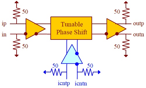
Fig. 1 Functional Block Diagram
This device is now considered obsolete and has been superceded by ASNT5106-PQC which can be found at the link below:
ASNT5001A-PQC is a clock / data variable delay line fabricated in a SiGe technology. The IC provides an adjustable delay of its differential output signal outp/outn in relation to its broadband input signal ip/in. The delay adjustment range is temperature-stabilized. The delay is controlled through a wide-band differential tuning port icntp/icntn.
The part’s I/Os support the CML logic interface with on chip 50Ω termination to vcc and may be used differentially, AC/DC coupled, single-ended, or in any combination. In the DC-coupling mode, the input signal’s common mode voltage should comply with specifications shown in the electrical characteristics table within the part’s datasheet. In the AC-coupling mode, the input termination provides the required common mode voltage automatically. The differential DC signaling mode is recommended for optimal performance, and the output buffer is linearized for reduction of undershoot and overshoot on the output waveforms. Due to an extremely low jitter, the part is suitable for use in high-speed test and measurement equipment.