Product Details
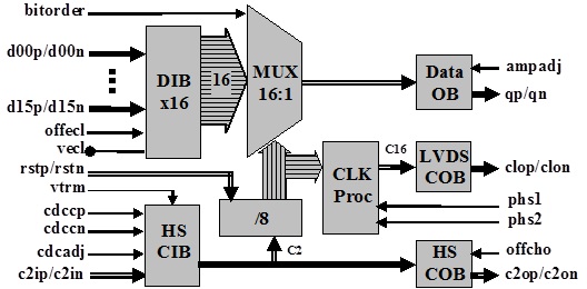
Fig. 1 Functional Block Diagram
ASNT1140-KMA is a high-speed DDR (dual data rate) digital 16-to-1 multiplexer (MUX) / serializer. The IC shown in Fig. 1 functions seamlessly over the specified range of data rates (fbit). The main function of the IC is to multiplex 16 parallel data channels running at a bit rate of fbit/16 into a high-speed serial bit stream running at fbit. It provides a high-speed output data channel for point-to-point data transmission over a controlled impedance media of 50Ohm. The transmission media can be a printed circuit board or copper coaxial cables. The functional distance of the data transfer is dependent upon the attenuation characteristics of the transportation media and the degree of noise coupling to the signaling environment.
During normal operation, the serializer’s data input buffer (DIBx16) accepts external 16-bit wide parallel data words d00p/d00n-d15p/d15n through 16 differential LVDS inputs and delivers them to the multiplexer’s core (MUX16:1) for serialization. A half-rate CML clock (a full-rate clock divided by 2) must be provided by an external source to the inputs c2ip/c2in of the high-speed clock input buffer (HS CIB) where it is routed to both the high-speed clock output buffer (HS COB) and the internal divider-by-8 (/8). The high-speed CML clock input buffer provides on-chip 50Ohm termination and is designed to be driven by devices with 50Ohm source impedance. The duty cycle of the internal clock c2 can be adjusted either through a single ended control pin cdcadj or through a dual control port cdccp/cdccn. The clock input buffer uses a separate positive supply vtrm for additional common mode voltage adjustment. The divider provides signaling for MUX16:1 and produces a divided-by-16 full-rate clock C16 for the low-speed LVDS-compliant clock output buffer (LVDS COB). The divider can be preset to a certain initial state using external CML signals rstp/rstn. The phase of the low-speed output clock clop/clon can be modified in 90° increments by utilizing pins phs1 and phs2 and the clock processing block (CLK Proc). By utilizing the pin bitorder, the serializer can designate either d00p/d00n or d15p/d15n as the MSB (most significant bit that is delivered first to the serial interface), thus simplifying the interface between the multiplexer and a preceding device.
The serialized words are transmitted as a differential signal qp/dn by a CML output buffer (Data OB). A half-rate CML clock c2op/c2on is transmitted by HS COB in parallel with the high-speed data. The clock and data outputs are well phase matched to each other resulting in very little relative skew over the operating temperature range of the device. Both output stages are back terminated with on-chip 50Ohm resistors. The chip uses a single +3.3V power supply and is characterized for operation from −25°C to 125°C of junction temperature.