
Product Details
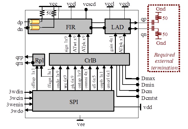
Fig. 1. Functional Block Diagram
The ASNT8172 is a differential driver with an externally controlled 9-tap pre-emphasis. It receives a high-speed binary data signal through its differential input port dp/dn. The FIR block processes the input signal in accordance with nine pre-defined filter coefficients to perform the pre-emphasis operation. The resulting analog signal is amplified by a linear amplifier-driver LAD, and delivered to the output linear differential port outp/outn that operates in ECL-type mode and requires external 50Ohm AC terminations. If DC terminations are desired, a special external resistor network should be designed. All chip functions are controlled through a 3-wire serial-to-parallel interface (SPI) that operates in combination with an internal control block CrlB. The chip includes a 1-tap replica Rpl that can be independently enabled and used for initial gain calibration as described below. The FIR block includes 8 dual transmission lines for direct and inverted input data signals with a single-ended impedance of 50Ohm and matching internal terminations to vcc at their ends. Signals from all 9 nodes are processed by tap buffers to deliver 9 delayed copies of the differential input signal with controlled signs and weights to a summation point. The signs and weights are defined by internal binary signals sign and analog signals ATwt respectively. In addition, frequency response (peaking) of each tap can be adjusted using internal analog signals ATpk. The weight of any tap #X can be reduced to exact 0 by a 1-bit digital signal ontapX=”0”, or can be controlled normally with ontapX=”1” as described below in CrlB. FIR requires initial calibration after which it delivers an optimal signal to its output. The calibration is performed using a replica block (Rpl) that is described below. LAD amplifies the analog signal from FIR, and delivers it to the differential output port outp/outn. This port operates in ECL-type mode as a current source/sink and requires external 50Ohm AC terminations. A DC termination scheme is also possible but requires an external resistor network. The gain and frequency response (peaking) of LAD can be adjusted using internal 4-bit binary signal gain, and six analog signals ADpk respectively. The LAD’s internal buffer with the gain adjust functionality includes a cascode stage for better performance. The reference voltage for the cascode stage can be monitored and adjusted through a control port vcscd to achieve the best output signal.