
Product Details
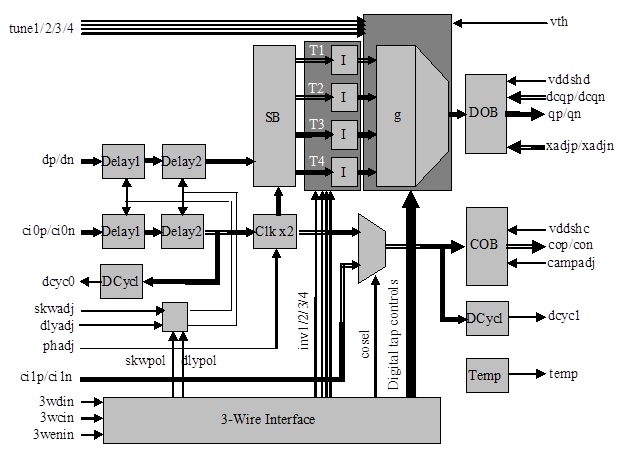
Fig.1 Functional Block Diagram
The ASNT6119B-KMF SiGe IC shown in Fig. 1 is an advanced programmable driver-amplifier (ADA) with built-in 4-tap pre-emphasis. The ADA generates a combination of four delayed copies of its input differential data signal dp/dn with certain user-controlled weights and polarities. The copies are created in a 4-bit shift register activated by the ADA’s internal high-speed clock signal (see Sampling Block and Taps). This clock signal is a copy of the main input clock ci0p/ci0n with either matching or doubled (multiplied-by-2) frequency. In the multiply-by-2 clock mode, the duty cycles of the input and internal clock signals are monitored, and the output duty cycle can be adjusted through the external control port phadj (see Clock Multiplier). For the part’s correct operation, the input data rate in Gbps should be equal to the internal clock frequency in GHz.
Input clock and data signals can be delayed in the same or opposite directions to ensure their correct phase relation at the inputs of the shift register and at the chip outputs (see Input Delay Section). The ADA can accept one additional clock signal ci1p/ci1n and deliver it to the output port cop/con instead of the main clock ci0p/ci0n, thus operating as a clock buffer (see Additional Input Clock and Clock Output Buffer).
The part’s I/Os support CML logic interface with on-chip 50Ohm termination to ground. External 50Ohm termination is also required. DC-coupling for data and clock output ports is strongly recommended. The input ports can use DC or AC coupling. Differential input clock and data are strongly recommended. Amplitude and peaking in the clock and data output signals can be externally adjusted. Both single-ended data output signals also have controlled DC common-mode levels and eye crossing points (see Data Output Buffer). All operational modes of the chip are controlled through a high-speed 3-wire serial interface (see 3-Wire Interface Control Block).
The chip operates from one negative power supply (positive pin connected to external Ground, negative pin vee = -4.3V) and one floating positive power supply (negative pin connected to vee and positive pin v3p5 = 3.5V). It is recommended to keep the relative deviation of v3p5 from Ground within less than ±0.1V.